Back Bandgaping Afrikaans فجوة النطاق Arabic Banda prohibida Catalan Bandlücke German Bendbreĉo Esperanto Banda prohibida Spanish Keelutsoon (füüsika) Estonian نوار ممنوعه Persian Bande interdite French פער אסור HE

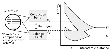
In solid-state physics and solid-state chemistry, a band gap, also called a bandgap or energy gap, is an energy range in a solid where no electronic states exist. In graphs of the electronic band structure of solids, the band gap refers to the energy difference (often expressed in electronvolts) between the top of the valence band and the bottom of the conduction band in insulators and semiconductors. It is the energy required to promote an electron from the valence band to the conduction band. The resulting conduction-band electron (and the electron hole in the valence band) are free to move within the crystal lattice and serve as charge carriers to conduct electric current. It is closely related to the HOMO/LUMO gap in chemistry. If the valence band is completely full and the conduction band is completely empty, then electrons cannot move within the solid because there are no available states. If the electrons are not free to move within the crystal lattice, then there is no generated current due to no net charge carrier mobility. However, if some electrons transfer from the valence band (mostly full) to the conduction band (mostly empty), then current can flow (see carrier generation and recombination). Therefore, the band gap is a major factor determining the electrical conductivity of a solid. Substances having large band gaps (also called "wide" band gaps) are generally insulators, those with small band gaps (also called "narrow" band gaps) are semiconductors, and conductors either have very small band gaps or none, because the valence and conduction bands overlap to form a continuous band.
It is possible to produce laser induced insulator-metal transitions which have already been experimentally observed in some condensed matter systems, like thin films of C60,[1] doped manganites,[2] or in vanadium sesquioxide V2O3.[3] These are special cases of the more general metal-to-nonmetal transitions phenomena which were intensively studied in the last decades.[4] A one-dimensional analytic model of laser induced distortion of band structure was presented for a spatially periodic (cosine) potential. This problem is periodic both in space and time and can be solved analytically using the Kramers-Henneberger co-moving frame. The solutions can be given with the help of the Mathieu functions.[5]
- ^ Phillips, H.M.; Sarkar, D.; Halas, N.J.; Hauge, R.H.; Sauerbrey, R. (1993). "Excimer-laser-induced electric conductivity in thin-film C60". App. Phys. A. 57: 105–107. doi:10.1007/BF00331226.
- ^ Hao, L; Wang, J; Xing, D.Y. (2006). "Photoinduced insulator-metal transition in the doped manganites Pr0.55(Ca0.75Sr0.25)0.45MnO3 and Pr0.7Ca0.3MnO3: Electronic structure from a self-consistent mean-field approach". Phys. Rev. B. 74: 0144440. doi:10.1103/PhysRevB.74.014440.
- ^ Abreu, E.; Siming, W.; Ramirez, G; Liu, M.; Zhang, J.; Geng, K.; Averitt, R.D. (2015). "Dynamic conductivity scaling in photoexcited V2O3 thin films". Physical Review B. 92 (8): 085130. arXiv:1410.6804. doi:10.1103/PhysRevB.92.085130.
- ^ Redmer, R.; Holst, B; F., Hensel (2010). Metal-to-Nonmetal Transitions. Springer.
- ^ Varró, S.; Földi, P.; Barna, I.F. (2018). "Laser induced distortion of band structure in solids: an analytic model". IOP Conf. Series: Journal of Physics: Conf. Series. 1206: 012005. arXiv:1812.04676. doi:10.1088/1742-6596/1206/1/012005.