Back Flitsgeheue Afrikaans ذاكرة وميضية Arabic Fləş-yaddaş Azerbaijani Флэш-памяць Byelorussian Флашпамет Bulgarian ফ্ল্যাশ মেমোরি Bengali/Bangla Flash memorija BS Memòria flaix Catalan Flash paměť Czech Flash-lager Danish

| Computer memory and data storage types |
|---|
| Volatile |
| Non-volatile |
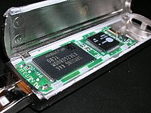
Flash memory is an electronic non-volatile computer memory storage medium that can be electrically erased and reprogrammed. The two main types of flash memory, NOR flash and NAND flash, are named for the NOR and NAND logic gates. Both use the same cell design, consisting of floating-gate MOSFETs. They differ at the circuit level depending on whether the state of the bit line or word lines is pulled high or low: in NAND flash, the relationship between the bit line and the word lines resembles a NAND gate; in NOR flash, it resembles a NOR gate.
Flash memory, a type of floating-gate memory, was invented by Fujio Masuoka at Toshiba in 1980 and is based on EEPROM technology. Toshiba began marketing flash memory in 1987.[1] EPROMs had to be erased completely before they could be rewritten. NAND flash memory, however, may be erased, written, and read in blocks (or pages), which generally are much smaller than the entire device. NOR flash memory allows a single machine word to be written – to an erased location – or read independently. A flash memory device typically consists of one or more flash memory chips (each holding many flash memory cells), along with a separate flash memory controller chip.
The NAND type is found mainly in memory cards, USB flash drives, solid-state drives (those produced since 2009), feature phones, smartphones, and similar products, for general storage and transfer of data. NAND or NOR flash memory is also often used to store configuration data in digital products, a task previously made possible by EEPROM or battery-powered static RAM. A key disadvantage of flash memory is that it can endure only a relatively small number of write cycles in a specific block.[2]
NOR flash is known for its direct random access capabilities, making it apt for executing code directly. Its architecture allows for individual byte access, facilitating faster read speeds compared to NAND flash. NAND flash memory operates with a different architecture, relying on a serial access approach. This makes NAND suitable for high-density data storage but less efficient for random access tasks. NAND flash is often employed in scenarios where cost-effective, high-capacity storage is crucial, such as in USB drives, memory cards, and solid-state drives (SSDs).
The primary differentiator lies in their use cases and internal structures. NOR flash is optimal for applications requiring quick access to individual bytes, like in embedded systems for program execution. NAND flash, on the other hand, shines in scenarios demanding cost-effective, high-capacity storage with sequential data access.
Flash memory[3] is used in computers, PDAs, digital audio players, digital cameras, mobile phones, synthesizers, video games, scientific instrumentation, industrial robotics, and medical electronics. Flash memory has a fast read access time but it is not as fast as static RAM or ROM. In portable devices, it is preferred to use flash memory because of its mechanical shock resistance since mechanical drives are more prone to mechanical damage.[4]
Because erase cycles are slow, the large block sizes used in flash memory erasing give it a significant speed advantage over non-flash EEPROM when writing large amounts of data. As of 2019,[update] flash memory costs greatly less than byte-programmable EEPROM and had become the dominant memory type wherever a system required a significant amount of non-volatile solid-state storage. EEPROMs, however, are still used in applications that require only small amounts of storage, e.g. in SPD implementations on computer memory modules.[5][6]
Flash memory packages can use die stacking with through-silicon vias and several dozen layers of 3D TLC NAND cells (per die) simultaneously to achieve capacities of up to 1 tebibyte per package using 16 stacked dies and an integrated flash controller as a separate die inside the package.[7][8][9][10]
- ^ Cite error: The named reference
:0was invoked but never defined (see the help page). - ^ "A Flash Storage Technical and Economic Primer". FlashStorage.com. 30 March 2015. Archived from the original on 20 July 2015.
- ^ "Flash Memory Guide" (PDF). Kingston Technology. 2012. MKF-283US. Archived (PDF) from the original on 19 October 2023. Retrieved 4 December 2023.
- ^ Bauer, Roderick (6 March 2018). "HDD vs SSD: What Does the Future for Storage Hold?". Backblaze. Archived from the original on 22 December 2022.
- ^ "Memory Module Serial Presence-Detect Introduction" (PDF). Micron Technology. TN-04-42. Archived (PDF) from the original on 26 July 2022. Retrieved 1 June 2022.
- ^ "Serial Presence Detect - Technical Reference" (PDF). Texas Instruments. January 1998. SMMU001. Archived (PDF) from the original on 4 December 2023.
- ^ Shilov, Anton (30 January 2019). "Samsung Starts Production of 1 TB eUFS 2.1 Storage for Smartphones". AnandTech. Archived from the original on 2 November 2023.
- ^ Shilov, Anton (5 December 2017). "Samsung Starts Production of 512 GB UFS NAND Flash Memory: 64-Layer V-NAND, 860 MB/s Reads". AnandTech. Archived from the original on 3 November 2023.
- ^ Kim, Chulbum; Cho, Ji-Ho; Jeong, Woopyo; Park, Il-han; Park, Hyun-Wook; Kim, Doo-Hyun; Kang, Daewoon; Lee, Sunghoon; Lee, Ji-Sang; Kim, Wontae; Park, Jiyoon; Ahn, Yang-lo; Lee, Jiyoung; Lee, Jong-Hoon; Kim, Seungbum; Yoon, Hyun-Jun; Yu, Jaedoeg; Choi, Nayoung; Kwon, Yelim; Kim, Nahyun; Jang, Hwajun; Park, Jonghoon; Song, Seunghwan; Park, Yongha; Bang, Jinbae; Hong, Sangki; Jeong, Byunghoon; Kim, Hyun-Jin; Lee, Chunan; et al. (2017). 11.4 a 512Gb 3b/Cell 64-stacked WL 3D V-NAND flash memory. International Solid-State Circuits Conference. San Francisco: IEEE. pp. 202–203. doi:10.1109/ISSCC.2017.7870331. ISBN 978-1-5090-3758-2. ISSN 2376-8606. S2CID 206998691.
- ^ Tyson, Mark. "Samsung enables 1TB eUFS 2.1 smartphones". Hexus. Archived from the original on 23 April 2023.