Back مقبس 370 Arabic Socket 370 Catalan Socket 370 Czech Sockel 370 German Socket 370 Greek Socket 370 Spanish Socket 370 Finnish Socket 370 French Socket 370 Hungarian Soket PGA 370 ID
 | |
| Release date | 1998 |
|---|---|
| Designed by | Intel |
| Type | PGA-ZIF |
| Chip form factors | Plastic pin grid array (PPGA) and Flip-chip pin grid array (FC-PGA and FC-PGA2) |
| Contacts | 370[1] |
| FSB protocol | AGTL+, AGTL |
| FSB frequency | 66, 100 and 133 MT/s |
| Voltage range | 1.05–2.1 V |
| Processor dimensions | 1.95 × 1.95 inches[2] (49.53 mm x 49.53 mm) |
| Processors | Intel Celeron Mendocino (PPGA, 300–533 MHz, 2.0 V) Intel Celeron Coppermine (FC-PGA, 533–1100 MHz, 1.5–1.75 V) |
| Predecessor | Slot 1 |
| Successor | Socket 423 |
This article is part of the CPU socket series | |
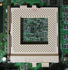
Socket 370, also known as PGA370, is a CPU socket first used by Intel for Pentium III and Celeron processors to first complement and later replace the older Slot 1 CPU interface on personal computers. The "370" refers to the number of pin holes in the socket for CPU pins.
Socket 370 was replaced by Socket 423 in 2000.
- ^ "CPU Sockets Chart". users.erols.com. Retrieved 2009-04-16.
- ^ "Intel Pentium III Specifications" (PDF).